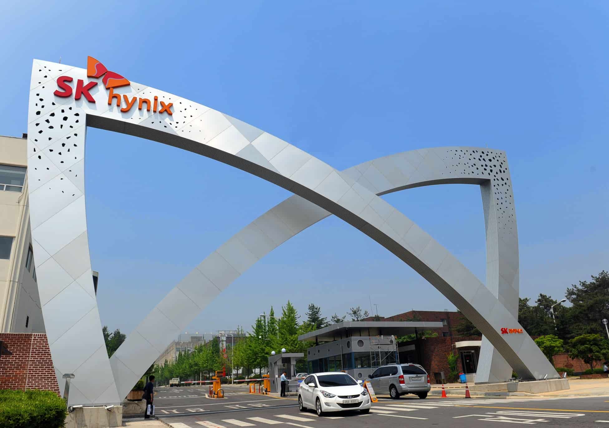
SK hynix announced the launch of the industry’s first high numerical aperture (High NA EUV) mass production lithography system at its M16 plant in Icheon, South Korea. The equipment, the ASML TWINSCAN EXE:5200B model, marks a milestone in the global semiconductor industry by enabling finer patterns and unprecedented transistor densities, essential for the next generation of DRAM memory and AI applications.
What is High NA EUV?
Extreme Ultraviolet Lithography (EUV) uses extremely short wavelengths of ultraviolet light to etch patterns on silicon wafers. The key to the new system is its numerical aperture (NA): while current EUV systems operate with an NA of 0.33, the EXE:5200B raises this to 0.55, representing a 40% improvement in optical precision.
This translates to:
- Transistor sizes 1.7 times smaller than with conventional EUV.
- 2.9 times higher densities, enabling more chips per wafer.
- Significant improvements in energy efficiency and device performance.
A decisive step in AI memory development
SK hynix, the second-largest memory manufacturer globally, aims to establish its leadership in next-generation memory for AI and computing. According to Cha Seon Yong, the company’s R&D head:
“We expect this critical infrastructure to turn our technological vision into reality. We aim to strengthen our leadership in AI memory with cutting-edge technology.”
The system will allow SK hynix to streamline previous EUV processes, accelerate the development of new DRAM generations, and enhance cost and performance competitiveness in a market driven by high demand from data centers, supercomputing, and machine learning applications.
Strategic partnership with ASML
The project is supported by the alliance with ASML, the Dutch lithography equipment manufacturer and the exclusive global supplier of EUV technology. According to Kim Byeong-Chan, the SK hynix-Japan customer team leader at ASML:
“High NA EUV is a critical technology that opens the next chapter in the semiconductor industry. We will work closely with SK hynix to drive innovation in next-generation memory.”
The system installation at the M16 plant was celebrated during an event attended by high-level executives from both companies, underscoring the strategic importance of this adoption.
Context: from 10 nm to 2 nm and beyond
Since 2021, SK hynix has been expanding its use of EUV in advanced memory production, starting with the 1anm node (fourth-generation 10 nm). The introduction of High NA EUV responds to the industry’s need to scale to extreme densities, in line with competitors like Samsung, TSMC, and Japanese Rapidus, which already plan to produce 2-nm chips by 2027.
SK hynix’s commitment aims to strengthen the stability and credibility of the global supply chain, bolstering its role as a strategic partner in providing high-value-added memory solutions.
Expected market impact
The arrival of commercial High NA EUV represents:
- Increased productivity: more DRAM chips per wafer and reduced costs.
- High-performance products: faster and more efficient memories for AI, big data, and cloud applications.
- Competitive edge: technological advantage over other manufacturers in an increasingly narrow-margin market.
- Supply chain resilience: technological diversification providing stability amid geopolitical tensions.
Conclusion
With the deployment of the first commercial High NA EUV system, SK hynix not only advances in the technological race but also lays the groundwork for a new era in DRAM memory, designed to meet the explosive growth in demand from AI and next-generation computing.
Frequently Asked Questions (FAQ)
What is High NA EUV lithography?
It’s an evolution of EUV lithography that enhances resolution by increasing the numerical aperture (NA), allowing for finer patterning and higher chip density.
What advantages does it have over conventional EUV?
It enables transistors 1.7 times smaller and densities 2.9 times higher, meaning more power, efficiency, and lower energy consumption.
Why is it key for DRAM memory?
Because it allows scaling memory cells to levels impossible with previous technologies, ensuring higher performance for AI, big data, and supercomputing.
What role does ASML play in this advancement?
ASML is the only EUV equipment manufacturer worldwide, and its EXE:5200B model is the first capable of providing High NA EUV for mass production.
via: SK Hynix News Notice

