Taiwan is investigating TSMC and Tokyo Electron employees for sharing images related to cutting-edge chip manufacturing processes, but industry sources claim the information isn’t sensitive.
The global semiconductor industry has been on edge in recent days following reports of a purported leak connected to Taiwan Semiconductor Manufacturing Company’s (TSMC) advanced 2-nanometer (nm) technology, the world’s leading chip manufacturer. However, insiders cited by DigiTimes downplay the severity: there’s no evidence of a critical intellectual property breach.
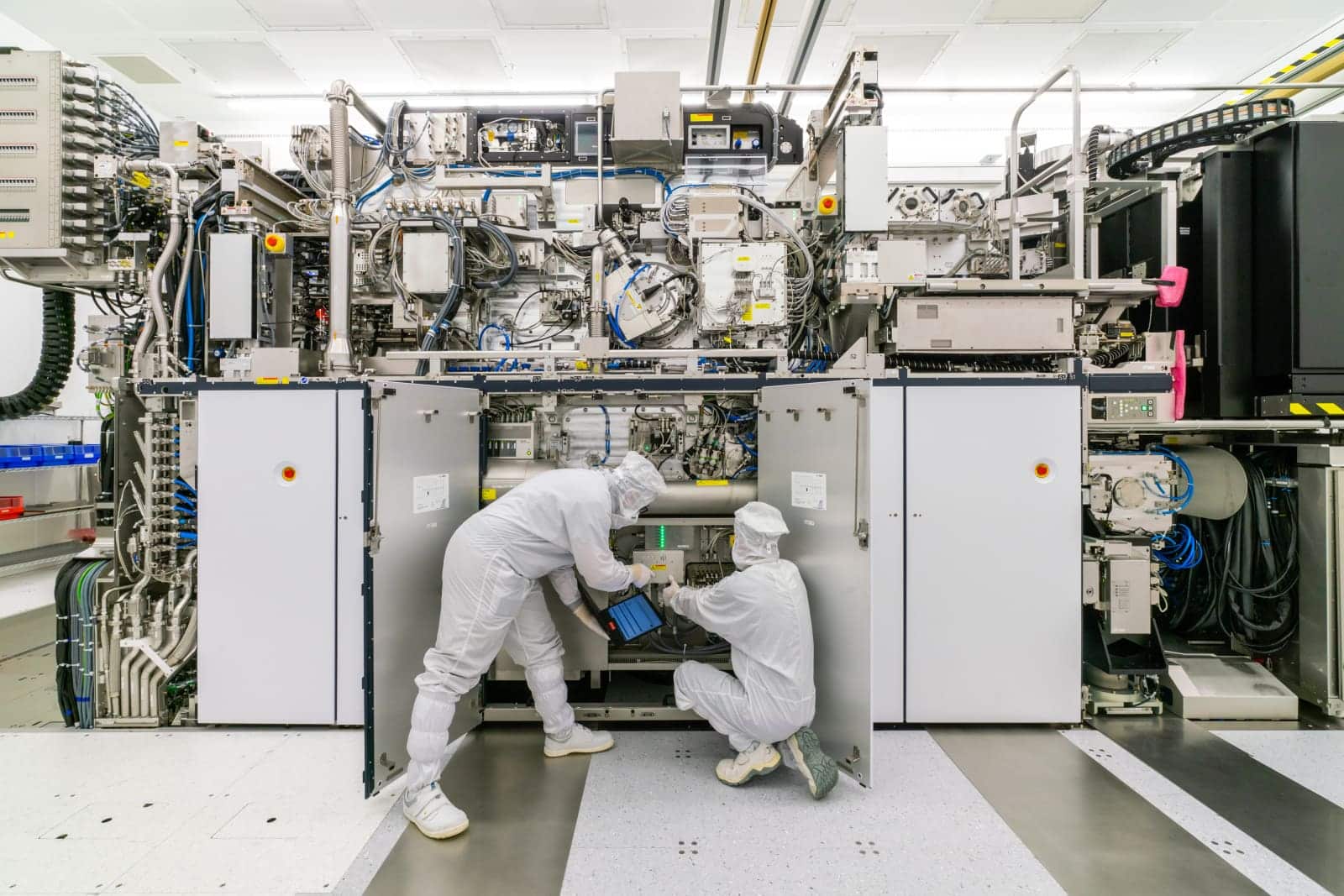
The incident unfolded when a lower-level TSMC employee at the Hsinchu Fab 20 plant— a key facility for future mass production of 2 nm nodes— was caught sharing photographs of control diagrams or wafer maps with an employee of Tokyo Electron, a Japanese lithography equipment supplier.
Both companies moved swiftly: the two employees were dismissed. Experts suggest the firings were likely more about setting an example than a response to an actual industrial espionage threat.
What was actually leaked?
According to the initial investigation, the shared information did not include circuit designs, algorithms, or R&D data. Instead, it consisted of images used to facilitate equipment installation tasks—operational documents, not strategic or proprietary data. There’s no indication that critical intellectual property or exclusive manufacturing technologies were compromised.
Tokyo Electron told Nikkei that “no confidential information has been identified as leaked,” while TSMC remains discreet, citing ongoing legal investigations.
A matter under national security scrutiny
Despite the limited technical scope of the leak, the case has escalated to Taiwan’s national security legal framework. Local prosecutors are investigating the individuals under laws that prohibit the transfer of sensitive technologies to regions like China, Hong Kong, or Macau.
This legal context underscores the enormous geopolitical importance of the semiconductor sector, especially for advanced processes like 2 nm, where only a few global players—TSMC, Intel, Samsung, and soon Rapidus—operate.
Who could benefit? No one, for now
Suspicion often falls on competitors like Huawei or SMIC, China’s leading foundry. However, DigiTimes sources agree that neither Huawei nor SMIC possess EUV lithography equipment—essential for manufacturing 2 nm chips.
Therefore, even if the shared data offered valuable clues, they wouldn’t be applicable without access to the appropriate technological infrastructure.
Regarding Rapidus, the new Japanese player collaborating with IBM on 2 nm technology, experts note that their processes differ fundamentally from TSMC’s, so technical compatibility is minimal.
Intel out of the picture
Another dismissed theory is Intel’s possible involvement. The U.S.-based manufacturer has been focusing on stabilizing its 18A node and has even indicated it might not offer it to external clients. For now, Intel’s priorities don’t include 2 nm technology, which remains in pre-production in their fabs.
A controversial firing goes viral
The scandal took a new turn when an X (formerly Twitter) user, known as Dr. Kim, claimed he was suspended and subsequently dismissed from TSMC after being linked to leak investigations. He said he received a legal notice with pending charges in Taiwan and planned to return to South Korea to avoid potential detention.
No official confirmation has linked his case directly to recent events, but the timing has rekindled debate on social media.
Context: The race for 2 nanometers
TSMC plans to begin volume production of 2 nm chips in 2025, employing an adopted GAAFET (Gate-All-Around Field Effect Transistor) architecture with nanosheets—an evolution of the current FinFET design. This node is expected to offer significant gains in energy efficiency and transistor density, critical for AI, advanced 5G, edge computing, and autonomous vehicles.
Hsinchu Fab 20 leads this effort, alongside future Fab 21 and Fab 22 in Taichung and Kaohsiung.
FAQs about the alleged TSMC leak
What exactly was leaked?
Internal photos of control diagrams or wafer maps, likely taken for maintenance or equipment setup. Designs, high-level secrets, or sensitive data weren’t exposed.
Why is 2 nm technology so important?
It represents the near future of high-performance semiconductors—smaller, faster, and more efficient chips. It’s a strategic advantage in the global tech rivalry.
Could Huawei or SMIC use this information?
No, because they lack EUV lithography tools needed for 2 nm manufacturing. Knowledge transfer without the necessary tech infrastructure isn’t an immediate competitive edge.
How did the involved companies respond?
TSMC and Tokyo Electron dismissed the employees involved and are cooperating with Taiwanese authorities. No significant damage or critical leakages have been reported.
What measures might TSMC implement moving forward?
Likely strengthened internal controls, especially in sensitive areas like advanced production facilities. Sharing knowledge selectively and enhancing digital traceability will be key strategies.
via: wccftech