The South Korean company is revolutionizing the industry with its TGV technology, aimed at AI applications and high-performance computing.
South Korean firm JNTC Co., Ltd. (KOSDAQ: 204270), which specializes in advanced materials, officially unveiled its new Glass Substrate with Through-Glass-Via (TGV) technology—a proprietary development designed to push beyond the limits of traditional plastic substrates in the semiconductor industry. The announcement was made during an event held at the Korea Exchange conference hall, attended by over 200 people, including journalists and investors.
Under the slogan “Carving Semiconductors in Glass, the Dream Material,” CEO Andrew Cho revealed technical details of the product, highlighting its application in artificial intelligence (AI) systems and high-performance computing (HPC). The new substrate offers superior flatness, thermal stability, and exceptional capabilities to minimize deformation and heat generation during high-speed processes.
Domestic Production with Proprietary Technology
JNTC completed its national manufacturing line in June and plans to begin volume production starting in August, after pilot tests in July. Unlike other industry players, JNTC has designed and built most of its key machinery in-house, allowing it to reduce initial investment costs to one-fifth of the industry average and maintain complete independence in the manufacturing process.
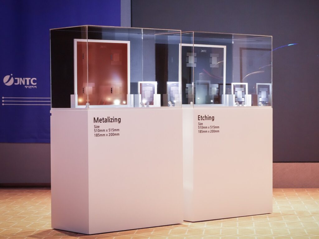
JNTC’s TGV glass substrates come in various sizes and thicknesses, featuring high-precision vias without microcracks (0%), as well as proprietary technologies for etching, bubble-free metallization, and finishing—achieving over 90% yields with minimal defects. Additional functions, such as alignment marks and cavities, have been verified through tests with major semiconductor manufacturers worldwide.
A Strategic Component for the New Packaging Era
“The TGV glass substrate is establishing itself as a crucial component in advanced packaging of next-generation semiconductors,” Cho stated during the presentation. “We have gained a clear competitive edge in quality and cost, and are currently working with 16 global partners in the semiconductor ecosystem.”
The company has also confirmed its plans to expand exports and build a large-scale manufacturing plant in Vietnam in the second half of the year, as part of its strategy to position itself as a key global player in precision materials for advanced packaging.
A Commitment to Glass Amid Technological Transition
JNTC’s launch occurs in a context where the use of glass as a base material is gaining traction in the semiconductor industry. Compared to traditional organic substrates, glass substrates offer better mechanical, thermal, and electrical properties, making them ideal for supporting increasingly complex chips used in AI, 5G, servers, and data centers.
The TGV technology, which involves drilling vertical vias in the glass to connect different circuit layers, is particularly relevant for 2.5D and 3D packaging systems that require high density, precision, and effective thermal dissipation.
With this announcement, JNTC not only demonstrates its innovative capacity but also takes a strategic stance in leading an emerging segment that will be vital for the evolution of chip design in the coming years.