The German company is ahead of the market following TSMC’s announcement of the shutdown of GaN production, positioning itself as a global leader in gallium nitride technology.
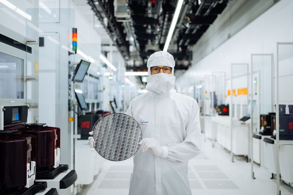
Infineon Technologies AG has confirmed that its roadmap for manufacturing gallium nitride (GaN) on 300 millimeter wafers is progressing as planned. The German multinational, operating under the IDM (Integrated Device Manufacturer) model, will offer the first samples to customers in the fourth quarter of 2025, thus reinforcing its role as a key player in the global advanced power components market.
This announcement comes at a strategic time: TSMC, the main competitor in the segment, has announced the cessation of its GaN production line and the dismantling of its facilities over the next two years. This move opens a significant window of opportunity for Infineon, making it the first manufacturer to successfully integrate 300 mm GaN technology into high-volume production infrastructure.
Efficiency and Scalability: Advantages of 300 mm Wafers
The transition from traditional 200 mm wafers to 300 mm represents a substantial technical and economic advancement. According to the company, this change allows for the production of up to 2.3 times more chips per wafer, significantly improving efficiency and contributing to cost parity with equivalent silicon-based products.
“With the full-scale manufacturing of GaN on 300 mm wafers, we will be able to deliver more value to our customers more quickly while progressing toward cost competitiveness against silicon,” stated Johannes Schoiswohl, Head of the GaN business line at Infineon. “Our IDM strategy and previous investments in infrastructure are paying off.”
A Comprehensive and Differentiated Approach
Infineon dominates the three key technologies in power semiconductors: silicon (Si), silicon carbide (SiC), and gallium nitride (GaN). This versatility, along with complete control over the production process—from design to final product—enables it to offer customized and scalable solutions for emerging applications in sectors such as:
- Electric automotive
- Energy systems for artificial intelligence
- Industrial robotics
- Solar inverters and motor controllers
- Fast chargers and smart adapters
GaN, in particular, stands out for its high power density, faster switching speeds, and lower energy losses, resulting in more compact designs that are thermally efficient.
A Market-Backed Commitment
According to a report from the Yole Group, the GaN power semiconductor market is set to grow at a rate of 36% annually, reaching a business volume of 2.5 billion US dollars by 2030. Infineon has already announced more than 40 new GaN-based products in the last 12 months, further solidifying its technological and industrial leadership.
With TSMC’s withdrawal from the GaN market—now focused on high-margin logic processors—Infineon strengthens its position as the preferred supplier for customers seeking high-reliability, scalable, and cost-competitive solutions.
Towards a New Era of Energy Efficiency
The integration of GaN technology on 300 mm wafers marks a turning point in the power semiconductor industry, accelerating the transition to devices that are more efficient, sustainable, and tailored to the new demands of the market, from smart homes to electric vehicles and AI data centers.
With solid manufacturing capabilities, a dedicated team of GaN experts, and one of the broadest intellectual property portfolios in the sector, Infineon positions itself as a European and global leader in the post-silicon era.
Source: infineon