The Taiwanese company will open eight wafer factories and one advanced packaging line to meet the growing demand for high-performance computing and artificial intelligence.
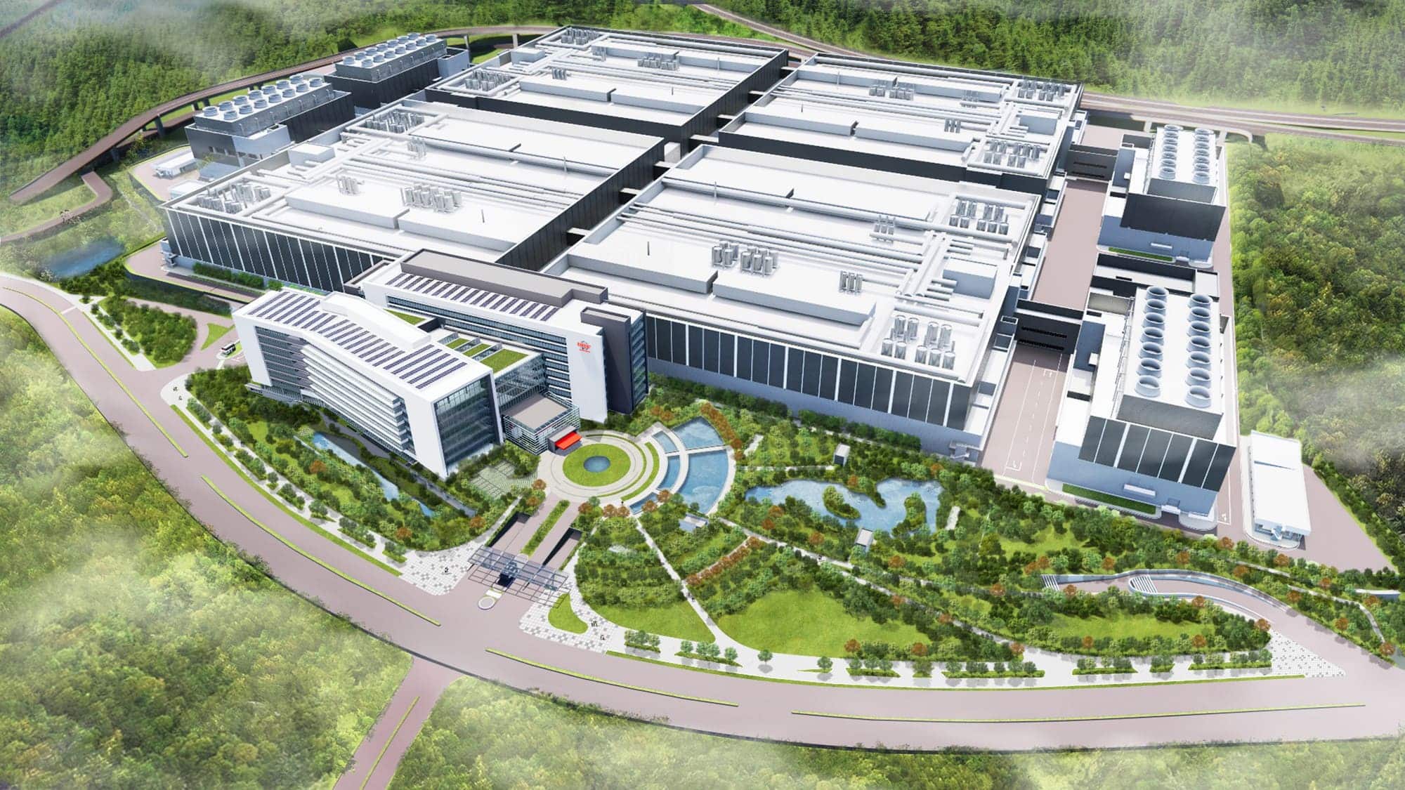
Taiwan Semiconductor Manufacturing Company (TSMC) has announced the largest expansion plan in its history for the year 2025, with the opening and equipping of up to nine advanced plants—eight wafer fabs and one chip packaging line known as CoWoS (Chip on Wafer on Substrate). This unprecedented deployment will be backed by a record investment of between $38 billion and $42 billion, according to company executives during their annual technology symposium.
This budget far exceeds the $29.2 billion allocated for 2024 and also surpasses the previous record of $35.2 billion in 2022, reflecting both the simultaneous volume of projects and the rising costs of lithography equipment, where each new low-NA EUV machine costs approximately $235 million, while high-NA models reach $380 million.
Strong Local and International Expansion
In its home country, Taiwan, TSMC is accelerating production on 2-nanometer (nm) nodes at Fabs 20 and 22, and preparing Fab 25 in Taichung for even more advanced nodes. In Kaohsiung, the company plans to build up to five new facilities that will house 2 nm, A16 (equivalent to 1.6 nm), and other next-generation technologies.
Outside of Taiwan, the expansion is also significant. In the United States, TSMC has completed the second phase of Fab 21 in Arizona, initiated the third phase, and is progressing on equipping a second factory in Kumamoto, Japan. In Europe, the city of Dresden, Germany, will host the new Fab 24 complex.
Demand for AI and HPC Drives Investment
The main driver behind this massive investment is the unstoppable demand for high-performance computing (HPC) and artificial intelligence (AI). AI-dedicated chips, such as training accelerators, require significantly larger silicon surfaces than traditional processors, forcing customers to request more wafers per design.
This growth has also strained advanced packaging capabilities, especially in CoWoS. TSMC now estimates a compound annual growth rate of 80% in CoWoS capacity between 2022 and 2025, well above the 60% it projected last year.
The Challenge: Meeting Deadlines
Meeting this ambitious timeline will depend on multiple factors: from construction milestones and machinery delivery to commercial adoption of advanced nodes like N2P and A16. Nevertheless, the 2025 plan makes it clear that TSMC aims to maintain its global leadership as a foundry, scaling its capacity in line with the increasing demand for chips.
With this strategy, TSMC is not only positioning itself to serve giants like Apple, NVIDIA, or AMD but also reinforcing its geostrategic role as a key supplier in the global context of the race for technological supremacy.
Source: Notebook check