A new breakthrough could revolutionize semiconductor manufacturing by addressing one of its biggest challenges: the precise alignment of layers in three-dimensional chips.
A team of researchers from the University of Massachusetts Amherst has developed an innovative technique based on lasers and metalenses that enables the alignment of 3D chip layers with unprecedented precision, achieving scales comparable to the size of an atom.
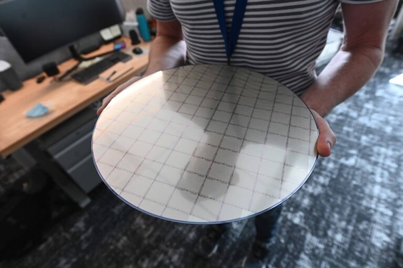
As electronic devices become more compact and powerful, the semiconductor industry has started to adopt three-dimensional designs, where multiple layers of two-dimensional chips are stacked. However, this architecture presents significant technical challenges, including the need for extremely precise alignment between layers. Even a slight misalignment can negatively impact chip performance.
Limitations of Current Methods
Traditionally, alignment is performed using microscopes that allow for the overlay of visual markers—such as crosses or corners—positioned on each layer. However, this method is limited by the distance between the layers (on the order of hundreds of microns) and the need for constant refocusing, which can cause additional displacements.
“The microscope cannot focus on both layers at the same time, and trying to do so can move the pieces and worsen the misalignment,” explained Maryam Ghahremani, the lead author of the study.
Additionally, the diffraction limit of optical microscopes restricts the minimum resolution to about 200 nanometers, preventing the detection of smaller misalignments.
A New Technique with Sub-Nanometer Precision
The method developed by the UMass Amherst team uses concentric metalenses as alignment markers. These metalenses—flat optical structures with advanced light manipulation capabilities—are embedded in each layer of the chip. By passing a laser through these markers, interferometric holograms are generated, the shape of which reveals whether the layers are correctly aligned.
“This interference image not only indicates whether the chips are aligned but also in what direction and by how much they are misaligned,” added Ghahremani.
The results exceeded initial expectations. Although the goal was to achieve a precision of 100 nanometers, the technique was able to detect misalignments as small as 0.017 nanometers in the horizontal axis and 0.134 nanometers in the vertical axis.
“We can detect if an object has shifted relative to another by a distance on the order of an atom,” emphasized Amir Arbabi, professor of electrical and computer engineering and senior author of the study.
Implications for the Semiconductor Industry
The precision achieved could represent a radical shift in chip manufacturing, where improper alignment poses a persistent technical and economic problem. Reducing this barrier would allow smaller companies and startups to access advanced manufacturing processes without relying on extremely expensive tools.
Furthermore, the researchers believe this technology could be applied to compact, low-cost sensors. “Many physical quantities can be translated into displacements. With a simple laser and a camera, we could develop pressure sensors, vibration detectors, or devices to monitor environmental changes,” stated Arbabi.
This advancement, beyond its relevance to the semiconductor industry, could pave the way for new generations of high-precision sensors for industrial, medical, and scientific applications.
Source: University of Massachusetts Amherst and Techspot