China continues to advance in the semiconductor industry despite the restrictions imposed by the United States. A team of researchers from Peking University, led by Professor Peng Hailin, has introduced the first silicon-free GAA 2D transistor, a revolutionary breakthrough that could change the future of chip manufacturing. Published in the journal Nature, the finding introduces a bismuth-based material that promises to exceed the capabilities of current transistors.
A Milestone in Transistor Evolution
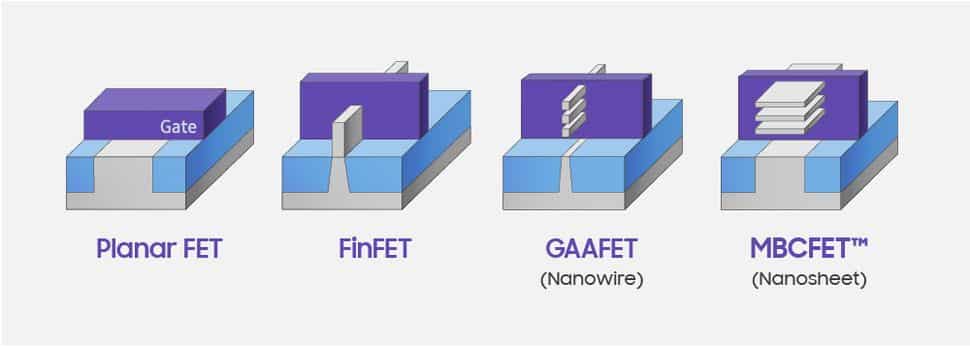
GAAFET (Gate-All-Around Field-Effect Transistor) transistors represent the evolution of traditional MOSFETs and FinFETs by allowing complete control over the conduction channel. However, until now, their development has been linked to the use of silicon. The innovation from the Chinese team lies in the use of Bi₂O₂Se (bismuth selenide oxide) as a semiconductor, achieving the first silicon-free GAA 2D configuration.
Professor Peng Hailin didn’t hesitate to describe this advancement as a turning point:
“This is the fastest and most efficient transistor ever created. If innovations in chips based on existing materials are considered a ‘shortcut,’ our development of transistors based on 2D materials is like a ‘lane change.’”
Comparison with Industry Leaders
The research team claims that their transistor outperforms current solutions from manufacturers like Intel, TSMC, and Samsung. Under similar operating conditions, the Chinese transistor demonstrated a 40% increase in performance and 10% better energy efficiency compared to TSMC’s N3B. This advancement could place it on par with advanced processes like TSMC’s N3X or even N2.

Advantages of the Silicon-Free GAA 2D Transistor
The use of Bi₂SeO₅ as a dielectric material allows the transistors to be more flexible and resilient, surpassing silicon in electron mobility. According to the study’s data, the new transistor presents an electron mobility of 280 cm²/Vs and a subthreshold swing of 62 mV/dec, very close to the ideal theoretical limit of 60 mV/dec.
This development implies significant benefits:
- Better integration with current CMOS architectures.
- Lower energy consumption in electronic devices.
- Greater integration density, optimizing power scaling.
Challenges and Large-Scale Viability
Despite its advantages, the adoption of this technology in the industry faces key challenges:
- Scalability and mass production: The manufacturing of wafers with this material and its integration into conventional lithographic processes have yet to be proven on a large scale.
- Production costs: Without a consolidated infrastructure for manufacturing silicon-free chips, initial costs could be high.
- Industrial compatibility: Though the transistor is compatible with CMOS architectures, its implementation will require changes in current manufacturing processes.
A Step Forward in the Global Technology Race
This advancement comes amid increasing technological restrictions imposed by the U.S. on China. With the ban on access to advanced tools like EUV lithography, China has opted for an alternative strategy: disruptive innovation. Instead of competing by the same rules, the Asian giant is developing technologies that could surpass the limitations of silicon.
While it’s still too early to determine if silicon-free GAA 2D transistors will be widely adopted, this discovery represents a significant step in the global technology race. The semiconductor industry is constantly evolving, and China has demonstrated that, despite restrictions, it continues to find ways to innovate and challenge Western dominance in this key sector.

