Samsung Electronics has announced its entry into the market for glass substrates for semiconductors, a key technology for the development of high-performance chips, particularly in the field of artificial intelligence (AI). This decision marks a strategic shift in the industry, as until now there have been no glass substrates commercially marketed on a large scale.
A Step Toward Semiconductor Innovation
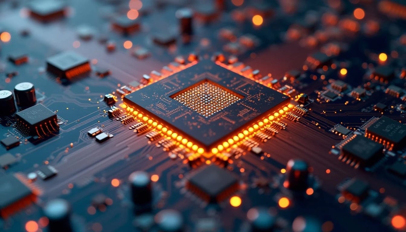
Glass substrates offer multiple advantages over traditional plastic substrates, as they allow for greater precision in circuit manufacturing and lower thermal deformation. These features make them particularly suitable for AI chips and other high-performance semiconductors.
To date, the development of this technology has been limited to initiatives from companies such as Intel, Appsolux, Samsung Electro-Mechanics, and LG Innotek. However, none of these companies had succeeded in implementing glass substrates on an industrial scale. By deciding to enter this market directly, Samsung aims to get ahead of its competitors and secure access to this crucial technology for the future of advanced computing.
Samsung’s Production Strategy
Samsung is establishing its own supply chain for the development of glass substrates, collaborating with specialized material, component, and equipment suppliers. While the company will lead technological development and design, the final manufacturing will be outsourced to third parties.
Industry sources have indicated that the company has already initiated technical discussions with various firms to ensure access to the necessary materials and processes. This strategy will allow Samsung to optimize production without directly assuming the challenges of large-scale manufacturing.
Challenges and Benefits of Glass Substrates
The development of glass substrates has historically been a challenge due to the fragility of the material and the difficulties in processing it. Any crack or impurity in the substrate can compromise the functionality of the semiconductor, which has hindered its adoption in the industry. However, their implementation offers significant improvements in performance, thermal dissipation, and circuit miniaturization.
Key advantages of glass substrates in semiconductors include:
- Greater precision in circuit manufacturing, enabling more compact and efficient chips.
- Lower thermal deformation, ideal for AI processors and high-performance chips.
- Increased potential to integrate more layers of circuits in the same space, optimizing the design of advanced chips.
Implications for the Semiconductor Market
Samsung’s entry into this market could have a significant impact on the semiconductor industry. Traditionally, the company has been a buyer of substrates, but with this move, it could become a supplier and direct competitor to companies specializing in the manufacturing of these materials.
Moreover, Samsung’s success in this segment could shift the market balance, affecting giants like Intel and AMD, which have also been exploring the use of glass substrates for their products.
If Samsung achieves mass production with competitive costs and high performance, it could become a key supplier for other companies, in addition to strengthening its position in the AI chip segment and semiconductor foundry.
The Future of Glass Substrates at Samsung
The company has avoided making official statements about this new project, but its strategy aims to solidify its position in advanced chip manufacturing. Furthermore, within the Samsung group, Samsung Electro-Mechanics was already working on the development of this technology, raising questions about the internal coordination between the two divisions.
With the growing demand for AI chips and high-performance semiconductors, Samsung’s bet on glass substrates could be a key move to secure its leadership in the tech industry in the coming years.
via: ETnews