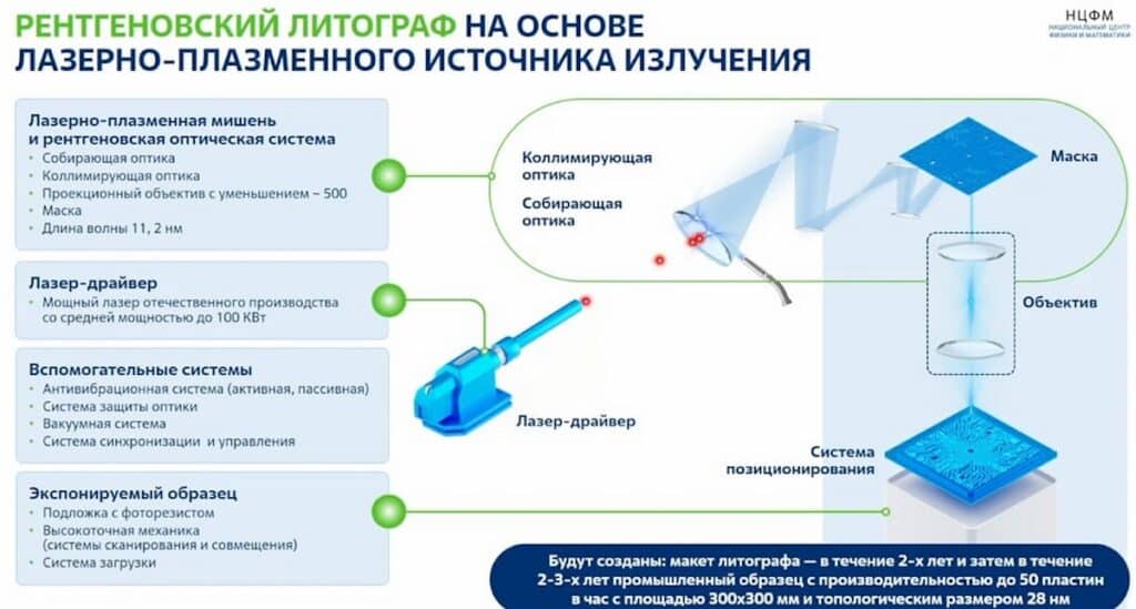
Russia has announced an ambitious project to develop EUV (extreme ultraviolet) scanners that promise to be more economical and easier to manufacture compared to advanced equipment from ASML, the global leader in this field. Led by the Institute of Microstructure Physics (IPM RAS), this effort aims to ensure Russia’s technological independence and position the country as a relevant player in emerging and less demanding markets.
Wavelength Reduction: An Innovative Approach
The key to this initiative lies in reducing the wavelength from 13.5 nm (used by ASML) to 11.2 nm, which improves resolution by 20% and significantly reduces production costs. According to Nikolay Chkhalo, the chief scientist at IPM RAS, using xenon sources instead of tin plasma will extend the lifespan of optical components and decrease operational costs. This shift also simplifies the production of mirrors and lenses, making them more accessible to smaller manufacturers.
Additionally, the Russian project will benefit from the use of organosilicon-based resists, which are better suited for the new wavelength, increasing the efficiency of manufacturing processes. Although the processing capacity will be less than ASML’s, these scanners are designed for smaller markets where cost and accessibility are crucial factors.
A Three-Stage Strategic Plan
The development of this technology is divided into three phases:
- Initial Research and Development: Focused on resolving key issues in EUV lithography technology and establishing cooperation links for the production of critical components.
- Functional Prototypes: Designing a scanner with key systems such as six-mirror lenses, high-power laser systems, and tools for 200/300 mm wafers. This step also includes integrating EUV lithography into advanced chip production chains.
- Mass Production: Developing equipment capable of processing over 60 300 mm wafers per hour, adapted for industrial applications and commercialization in global markets.

A Pragmatic Approach Against the ASML Giant
Russia has chosen not to replicate ASML’s model, which is extremely costly and complex. According to Chkhalo, ASML’s strategy has been successful due to the integration of the best global achievements, a difficult approach for a single country to emulate. Instead, Russia aims to create a more affordable and accessible alternative tailored to the needs of companies outside the current top 5 in the global chip market.
The project aims to achieve a 7 nm topology by 2028, with gradual progress starting with chip production at 350 nm in 2024 and 130 nm in 2026.
Challenges and Opportunities
Although the project is ambitious, it faces significant challenges such as the lack of specialists in Russia and high initial costs. According to Evgeny Gornev from the Moscow Institute of Physics and Technology, the Russian industry lacks skilled personnel and resources comparable to ASML, which invested three times more in R&D in 2022 than the entire budget projected for this effort in Russia.
However, the successful implementation of this roadmap could position Russia as a viable competitor in smaller and less demanding markets, offering a more affordable solution in a sector dominated by players like ASML, Nikon, and Tokyo Electron. Furthermore, this advancement would strengthen the country’s technological independence against international sanctions.
Global Impact
While the United States and Japan have failed to develop competitive EUV scanners, Russia is confident in its alternative approach. If successful, Russian technology could change the landscape of advanced lithography, providing access to cutting-edge tools for companies that currently cannot afford ASML equipment. This project, although risky, could redefine the global semiconductor industry.
via: Cnews.ru

