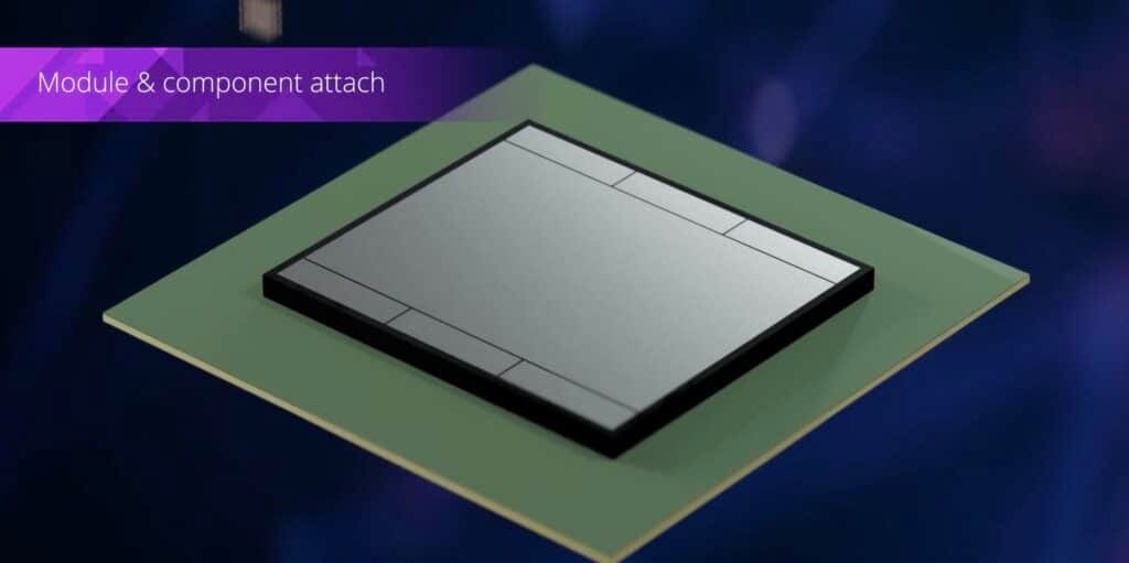
Amkor Technology has taken a step forward in the semiconductor industry with the development of its innovative S-SWIFT™ packaging technology. This new solution promises to transform the way advanced chips are manufactured and connected, offering significant improvements in performance and efficiency.
The challenge of smaller nodes
As the semiconductor industry moves towards increasingly smaller silicon technology nodes, currently at 3 nanometers, costs and development times have skyrocketed. Amkor engineers have identified that the smaller the node size, the higher the risk of defects, resulting in lower wafer yields.
Chiplet technology as a solution
To address these limitations, the industry has turned to chiplet technology. This approach allows for separating core blocks into smaller chips, thereby improving wafer performance and reducing design costs. However, interconnecting these heterogeneous chips requires advanced Integrated Circuit (IC) packaging technologies.
S-SWIFT: Amkor’s response
Amkor’s S-SWIFT (Substrate Silicon Wafer Integrated Fan-out Technology) technology stands out in the high-density packaging landscape. It provides increased bandwidth and chip-to-chip connections for heterogeneous integration with a high-density interposer.
Key features of S-SWIFT:
- Ultra-thin interface and µ-bump
- Precise control of deformation during thermal assembly
- Capillary fill and overmolding techniques
- Mold side ball formation process
ETR technology: The heart of S-SWIFT
One of the key innovations in S-SWIFT is the Embedded Trace Routing (ETR) redistribution layer process. This method addresses challenges in high-density Redistribution Layer (RDL) manufacturing, crucial for interconnecting chips with smaller node blocks.
The ETR process involves embedding the trace in the dielectric layer without an etching process, which solves issues like seed layer under etching and side etching concerns. The dual damascene copper structure in the ETR process offers advantages in high-frequency signal trace characteristics.
Proven reliability and performance
Amkor engineers have subjected the ETR structure in the S-SWIFT package to rigorous reliability testing. The seed layer surrounding the three sides of the ETR acts as a barrier, preventing copper ion migration and ensuring reliability under current, heat, and humidity conditions.
The future of Integrated Circuit packaging
With S-SWIFT, Amkor Technology is positioning itself at the forefront of IC packaging technology. This innovation promises to meet the growing demands of artificial intelligence applications, high-performance computing, and data centers.
As the industry continues to push the boundaries of silicon technology, innovations like S-SWIFT will play a crucial role in shaping the future of high-performance computing.
Source: amkor