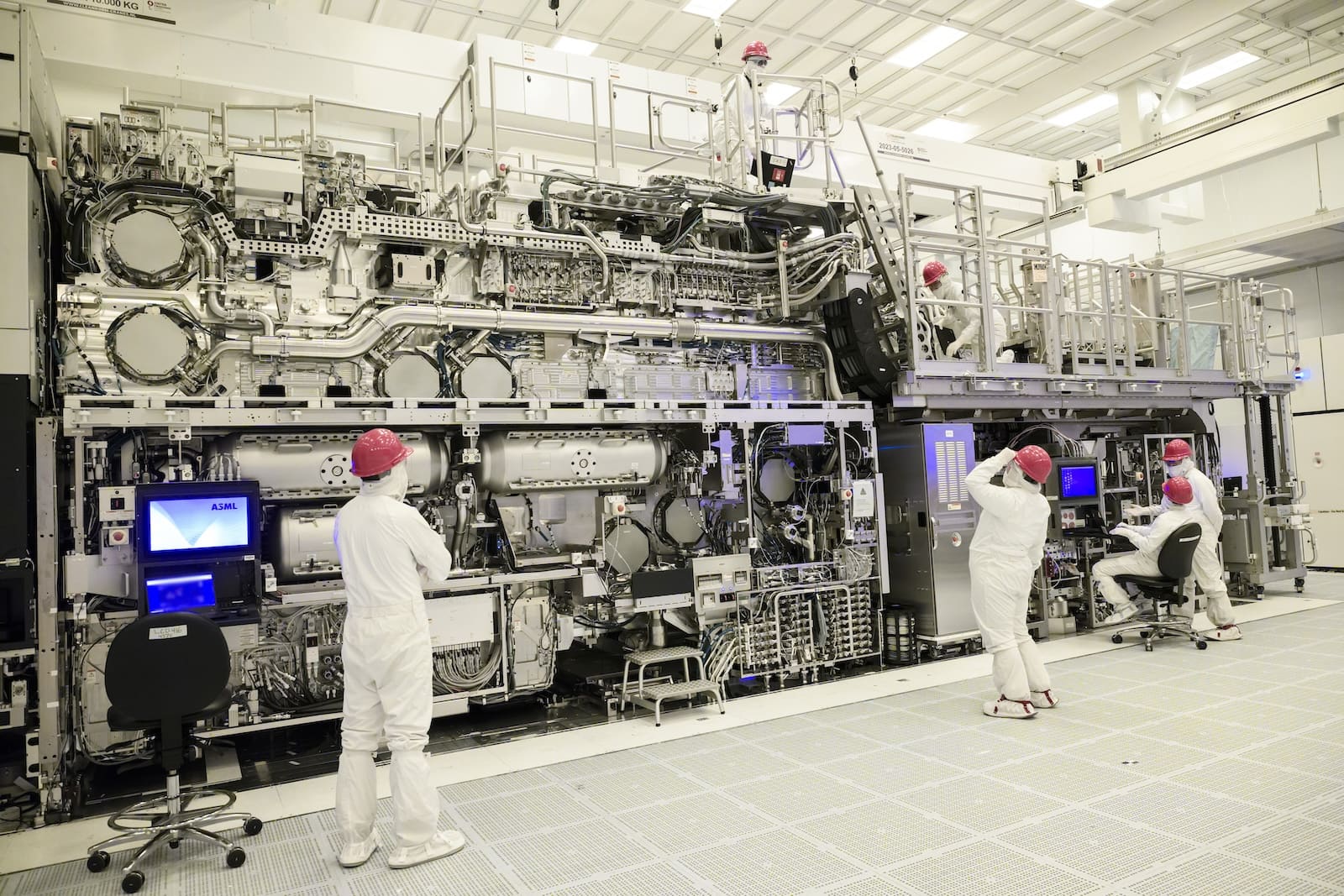
Intel Foundry Services has reached a significant milestone in the field of semiconductor manufacturing with the installation and calibration of the first high numerical aperture (High NA) extreme ultraviolet (EUV) lithography system in the industry. This breakthrough, located at its R&D site in Hillsboro, Oregon, promises to revolutionize the production of next-generation processors, marking a significant step forward in the miniaturization of electronic components.
A Leap Into the Future with High NA EUV
The TWINSCAN EXE:5000 High NA EUV system, developed by ASML, allows Intel not only to maintain but also extend its leadership in the semiconductor processing technology beyond its current Intel 18A process. This technology, resulting from decades of collaboration between Intel and ASML, is distinguished by its ability to dramatically improve resolution and feature scaling in chip manufacturing, essential for advancements in areas like artificial intelligence and other emerging technologies.
Why High NA EUV is Important
The use of High NA EUV technology is crucial for the development of advanced chips and the production of next-generation processors. This system offers unprecedented precision and scalability in chip manufacturing, enabling the creation of components with the most innovative features. Additionally, this tool has set a new world record by printing the finest lines observed to date – 10 nanometers of density at ASML facilities in Veldhoven, the Netherlands.
Implications of the New Technology for Intel and the Industry
With the implementation of High NA EUV, Intel not only solidifies its position in the semiconductor market but also sets new foundations for the future of microprocessor manufacturing. It is expected that this technology, combined with other Intel manufacturing processes, will enable the production of chips up to 1.7 times smaller than current ones, resulting in density up to 2.9 times higher.
The development of High NA EUV represents a significant step towards the era of angstroms, a period that will see Intel and the industry at large progress in chip miniaturization and capability, essential to support the growing demands of advanced technologies and energy-efficient consumption.
A Continued Commitment to Innovation and Development
Intel has demonstrated its commitment to research and development through substantial investments, such as the expansion of its D1X plant in Oregon. This facility, expanded with an investment of over $3 billion, not only strengthens Intel’s R&D infrastructure but also contributes to the economic and technological growth of the United States, aligning with national security and economic goals.
The adoption of High NA EUV technology places Intel at the forefront of Moore’s Law scaling, promoting a new generation of semiconductor technology and manufacturing in the U.S. and positioning the company to accelerate the next era of semiconductor technology.